
PCB Fabrication Assembly Is Used in Medical Devices
Medical devices are among the most complex and delicate electronic equipment, ranging from medical equipment used by doctors to life-saving implants in patients. Since they are directly linked to a patient’s well-being, they must meet strict and exacting standards that are enforced by regulatory bodies. This includes the PCB assembly process which has to follow precise manufacturing processes.
In order to ensure that the board meets the stringent requirements of medical equipment, the PCB must pass a number of tests and inspections. These include ensuring that the components are positioned accurately on the board and that the circuitry is free from defects such as shorts and unintended connections. This is why a CM should have a robust testing and inspection procedure for medical PCBs.
For example, a good CM will test for surface finishes to make sure that they are consistent and not damaged. They will also check the quality of the soldering and inspect for defects in the conductive materials. This is because any imperfections may compromise the safety of a patient’s health.
A medical device that contains a poorly assembled or defective PCB is not safe and could result in injury or even death. This is why it is essential for the CM to adhere to strict quality controls and document each step of their manufacturing process. In addition to this, they should also follow industry standards such as ISO 13485 and IEC 60601 which cover various aspects of medical equipment including electromagnetic compatibility and electrical safety.
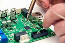
How PCB Fabrication Assembly Is Used in Medical Devices
Before the assembling process begins, the circuit board is cleaned to remove any contaminants that might affect its functionality. This is because contaminants can cause corrosion that will shorten the life of the circuit board or even affect the performance of the medical device that it is attached to.
The next step is layer alignment. This involves the laying out the inner and outer layers of the circuit board, using the holes from the previous stage as guides. After this, the copper layer is added. This can either be in the form of copper foil or a full-on copper coating. The purpose of this layer is to carry signals throughout the board, just like your nervous system carries signals between your brain and your muscles.
After the copper layer is in place, it is covered with a protective plastic called polyimide. This protects the copper from contamination and allows it to conduct more efficiently. This layer is also etched and laminated to create a rigid anchor for the components, which improves their stability and reliability.
Once the layer alignment is complete pcb fabrication assembly, the CM can start to assemble the parts. This requires specialized SMT (surface mount technology) equipment such as an automatic pick and place machine, a reflow oven, a wave soldering machine and AOI equipment. The CM will also need to have a first-article tester and an x-ray inspection machine.
The final step of the process is continuity testing, which can be done with automated testing equipment such as a bed of nails test fixture or flying probe test systems. This checks for unintentional shorts between nets, which would invalidate the finished product.